


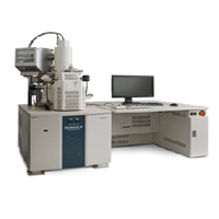
HITACHI 전자현미경
SU5000
주요특징
- Max. probe current is 200nA
- Ultra efficient photodiode BSE Detector, unmatched Low kV imaging to 100 V, and high probe current (>200 nA) for efficient microanalysis. - Variable Pressure - Unparalleled low vacuum (10-300 Pa) imaging with the novel Ultra Variable pressure Detector (UVD).
- Versatile analytical specimen chamber
- Quick and easy specimen exchange via stage drawer (Max. sample size : 200 mm dia. X 80 mmH) Microanalysis - EDS, WDS and EBSD, etc - Ultra-high resolution 3.0 nm at 15kV, 2.0 nm at 1kV
- Ultra-high resolution is available according to field proven Hitachi's semi-in-lens technique. - EM Wizard : Easy of use and Throughput
- Innovative "EM Wizard" GUI offers point-and-click optimized imaging.
- Groundbreaking computer-assisted technology offers a new level of SEM operation and control - Intuitive user interface
- Standard mode offers simple and quick operation.
Novice users are guided step by step and learn along the way thanks to the interactive user guide.
제품사양(Specification)
| (1) Resolution |
|---|
| 1.2 nm at 30kV / 3.0 nm at 15kV / 3.0 nm at 1kV 2.0 nm at 1kV with deceleration mode |
| (2) Magnification |
| 10~600,000x (baced on 4" x 5" picture), 30~1,500,000x (1,280x960 pixels on display) |
| (3) Accelerating voltage |
| 0.5 to 30kV (0.1kV step) |
| (4) Bias system |
| > 200nA |
| (5) Detectors |
| Everhart Thornley Secondary Electron Detector |
| (6) Low Vacuum Range |
| X : 0 ~ 100 mm Y : 0 ~ 50 mm Z : 3 ~ 65 mm T : -20 ~ 90 ˚ R : 360 ˚ |
| (7) Maximum loading sample size : Up to 200mm dia. (200mm dia. : option) |
| Maximum 80 mm height |
| (8) Image saving |
| Max. 5,120 x 3,840 pixels |
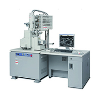
SU6600
주요특징
- Max. probe current is 200nA
- Various application including EDX, WDX, EBSP is used enoughly - Low vacuum mode standard built-in (ADAPT function)
- The useful function in observation and analysis of non-conductive samples is built-in.
- It's possible to exchange between high vacuum and low vacuum by only GUI controls. - Not only HR SE imaging but also BSE imaging from newly high sensitivity detector is observable.
- Additional ESED detector enables SE imaging in low vacuum. - Newly designed specimen chamber and specimen exchange chamber.
- Large chamber enables to attach EDX/WDX/EBSP and to analysis simultaneously.
- Max. sample size : 150mm dia. X 40mm H
제품사양(Specification)
| (1) Resolution |
|---|
| 1.2nm at 30kV / 3.0nm at 1kV (SE in high vacuum) 3.5nm at 30kV (BSE in low vacuum, 10Pa) |
| (2) Magnification |
| x10 to x600,000 (continuous) |
| (3) Accelerating voltage |
| 0.5 to 30kV |
| (4) 1pA to 200nA |
| 1pA to 200nA |
| (5) Anode heating system / Aperture heating system (HITACHI patent) |
| (6) Detectors |
| Everhart Thornley Secondary Electron Detector High sensitivity Backscattered Electron Detector Environmental Secondary Electron Detector (option) Transmitted Electron Detector (option) |
| (7) Variable pressure range |
| 10Pa to 300Pa |
| (8) Vacuum mode change |
| ADAPT function built-in |
| (9) Maximum loading sample size |
| 150mm dia. X 40mm H |
| (10) Image saving |
| Max. 5,120 x 3,840 pixels |
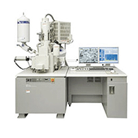
SU-70
주요특징
- Large probe current of 100nA
- Probe current up to 100nA available from the newly developed Schottky emission electron source. - Versatile analytical specimen chamber
- Multiple ports have been prepared for large variety of applications.
- Simultaneous analysis options : EDX, WDX, EBSP, STEM, BSE, CL, Cryo stage, Chamberscope. - Field Free mode (FF mode)
- FF mode for the imaging of magnetic samples and EBSP in a UHR SEM. - Ultra-high resolution 1.0nm at 15kV, 1.6nm at 1kV
- Ultra-high resolution is available according to field proven Hitachi's semi-in-lens technique. - Super E x B for controlled SE/BSE signal detection
- Reduction of charge-up effect in the image and signal filtering. - Ultra-low landing voltage for shallow surface observation
- Beam deceleration technology enables high resolution ultra-low voltage imaging.
제품사양(Specification)
| (1) Resolution |
|---|
| 1.0nm at 15kV / 1.6nm at 1kV |
| (2) Magnification |
| LM mode - x25 to x2,000 HM mode - x100 to x800,000 |
| (3) Accelerating voltage |
| 0.1 to 30kV |
| (4) Bias system |
| 1pA to 100nA |
| (5) Anode heating system / Aperture heating system (HITACHI patent) |
| (6) Detectors |
| Everhart Thornley Secondary Electron Detector Backscattered Electron Detector (option) STEM Detector (option) |
| (7) Specimen stage |
| X : 0 to 110mm Y : 0 to 110mm Z : 1.5 to 40mm R : 360˚ T : -5˚ to +70˚ Maximum sample size : 150mm dia. (200mm dia. : option) |
| (8) Pumping system |
| I.P x 2 + TMP x 1 + R.P x 1 |
| (9) Image saving |
| Max. 5,120 x 3,840 pixels |