


HITACHI 전자현미경
SU8010
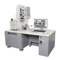
주요특징
- Ultra-high resolution imaging, even at ultra low accelerating voltage (SE resolution 1.3nm at 1.0kV)
- A wide range of signal detection systems
- User-friendly GUI, console and wide-format monitor for comfortable operation
- Wide range of optional accessories to meet customer-specific needs SU8010 has excellent performance as the entry level model in the SU8000 series. The combination of Semi-in-lens type objective lens and cold FE-gun with small energy spread delivers ultra resolution imaging performance and flexible SE-BSE signal mixing using Hitachi's detector technology for absolute surface information. Z-number contrast and charge suppression.
제품사양(Specification)
| (1) Resolution |
|---|
| 1.0nm at 15kV / 1.3nm at 1kV |
| (2) Magnification |
| On photo mode - x20 to x800,000 On display mode - x60 to x2,000,000 |
| (3) Accelerating voltage |
| 0.1 to 30kV |
| (4) Anode heating system / Aperture heating system (HITACHI patent) |
| (5) Detectors |
| Dual Secondary Electron Detector (Upper/Lower) SE/BSE Signal Mixing Function (Upper detector) Semiconductor type BSED (option) YAG type BSED (option) STEM detector for BF/DF-STEM (option) BF-STEM aperture (option) Cathodoluminescence Detector (option) EBIC image observation unit (option) |
| (6) Maximum loading sample size |
| 100mm dia. / 150mm dia.(option) |
| (7) Image saving |
| Max. 5,120 x 3,840 pixels |
SU8220/30/40
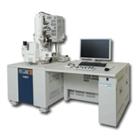
주요특징
- The ultimate SEM source for high resolution imaging at low acceleration voltage with unmatched beam brightness and stability
- The newly designed Hitachi CFE gun complements the inherent high resolution and brightness of conventional CFE with increased probe current and beam stability
- Long-term, continuous operation and elemental analysis are now routine with the new CFE source
- The beam decelertion voltage can be optimized to yield a landing voltage of 10-2000V enabling the observation of beam sensitive samples, such as organic materials or polymers, in the natural state without beam damage or sample deformation
- A new selective energy filtering system for the top detector offers fine contrast differentiation even at low accelerating voltages
제품사양(Specification)
| (1) Resolution |
|---|
| 0.8nm at 15kV / 1.1nm at 1kV |
| (2) Magnification |
| 0.8nm at 15kV / 1.1nm at 1kV |
| (3) Accelerating voltage |
| 0.01 to 30kV |
| (4) Anode heating system / Aperture heating system (HITACHI patent) |
| (5) Detectors |
| Triple Secondary Electron Detector (Top/Upper/Lower) SE/BSE Signal Mixing Function (Upper detector) Top filter function (Top detector)* Semiconductor type BSED* YAG type BSED* STEM detector for BF/DF-STEM* BF-STEM aperture* |
| (6) Image saving |
| Max. 5,120 x 3,840 pixels |
SU9000
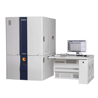
주요특징
- Superior low-kV performance for observation of beam sensitive materials.
- Next generation Hitachi In-lens SEM optics allows for routine observation at 1 million times.
- Newly designed CFE GUN provides high brightness and extremly stable emission current.
- Improved vacuum technology that allows for ultra-high vacuum levels for reduced sample contamination.
- Highly engineered instrument enclosure featuring both superior strength and stability to allow for high resolution imaging in a broad range of environmental conditions
- Newly designed objective lens provides for high resolution imaging at low acceleration voltage.
- Side entry sample exchange system increases throughput by reducing the time required to change samples and by automatically positioning the sample at the correct WD.
제품사양(Specification)
| (1) Resolution |
|---|
| 0.4nm at 30kV (Sample height = 1.0mm) 1.2nm at 1kV (Sample height = 2.0mm) |
| (2) Magnification |
| On photo mode - x80 to x3,000,000 On display mode - x220 to x8,000,000 |
| (3) Accelerating voltage |
| 0.5 to 30kV |
| (4) Anode heating system / Aperture heating system (HITACHI patent) |
| (5) Detectors |
| Secondary Electron Detector Top detector (option) BF/DF Duo-STEM Detector (option) |
| (6) Image saving |
| Image saving |